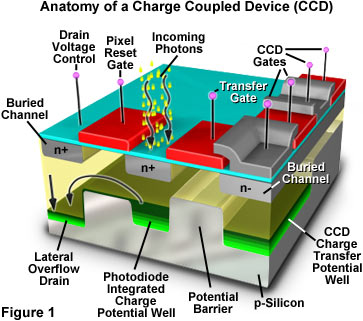
Charge-coupled devices (CCDs) are silicon-based integrated circuits consisting of a dense matrix of photodiodes that operate by converting light energy in the form of photons into an electronic charge. Electrons generated by the interaction of photons with silicon atoms are stored in a potential well and can subsequently be transferred across the chip through registers and output to an amplifier. The schematic diagram illustrated in Figure 1 shows various components that comprise the anatomy of a typical CCD.

CCDs were invented in the late 1960's by research scientists at Bell Laboratories, who initially conceived the idea as a new type of memory circuit for computers. Later studies indicated that the device, because of its ability to transfer charge and the photoelectric interaction with light, would also be useful for other applications such as signal processing and imaging. Early hopes of a new memory device have all but disappeared, but the CCD is emerging as one of the leading candidates for an all-purpose electronic imaging detector, capable of replacing film in the emerging field of digital photomicrography.
Fabricated on silicon wafers much like integrated circuits, CCDs are processed in a series of complex photolithographic steps that involve etching, ion implantation, thin film deposition, metallization, and passivation to define various functions within the device. The silicon substrate is electrically doped to form p-type silicon, a material in which the main carriers are positively charged electron holes. Multiple dies, each capable of yielding a working device, are fabricated on each wafer before being cut with a diamond saw, tested, and packaged into a ceramic or polymer casing with a glass or quartz window through which light can pass to illuminate the photodiode array on the CCD surface. Explore the sequence of steps necessary to build a CCD using our interactive Java tutorial, which is linked from the dialog box.
Building A Charge-Coupled Device
Explore the steps utilized in the construction of a charge-coupled device (CCD) as a portion of an individual pixel gate is fabricated on a silicon wafer simultaneously with thousands or even millions of neighboring elements.
When a ultraviolet, visible, or infrared photon strikes a silicon atom resting in or near a CCD photodiode, it will usually produce a free electron and a "hole" created by the temporary absence of the electron in the silicon crystalline lattice. The free electron is then collected in a potential well (located deep within the silicon in an area known as the depletion layer), while the hole is forced away from the well and eventually is displaced into the silicon substrate. Individual photodiodes are isolated electrically from their neighbors by a channel stop, which is formed by diffusing boron ions through a mask into the p-type silicon substrate.
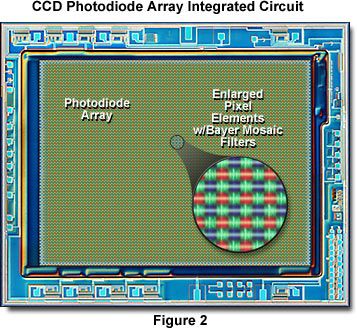
The principal architectural feature of a CCD is a vast array of serial shift registers constructed with a vertically stacked conductive layer of doped polysilicon separated from a silicon semiconductor substrate by an insulating thin film of silicon dioxide (see Figure 2). After electrons have been collected within each photodiode of the array, a voltage potential is applied to the polysilicon electrode layers (termed gates) to change the electrostatic potential of the underlying silicon. The silicon substrate positioned directly beneath the gate electrode then becomes a potential well capable of collecting locally-generated electrons created by the incident light. Neighboring gates help to confine electrons within the potential well by forming zones of higher potentials, termed barriers, surrounding the well. By modulating the voltage applied to polysilicon gates, they can be biased to either form a potential well or a barrier to the integrated charge collected by the photodiode.
The most common CCD designs have a series of gate elements that subdivide each pixel into thirds by three potential wells oriented in a horizontal row. Each photodiode potential well is capable of holding a number of electrons that determines the upper limit of the dynamic range of the CCD. After being illuminated by incoming photons during a period termed integration, potential wells in the CCD photodiode array become filled with electrons produced in the depletion layer of the silicon substrate. Measurement of this stored charge is accomplished by a combination of serial and parallel transfers of the accumulated charge to a single output node at the edge of the chip. The speed of parallel charge transfer is usually sufficient to be accomplished during the period of charge integration for the next image.
After being collected in the potential wells, electrons are shifted in parallel, one row at a time, by a signal generated from the vertical shift register clock. The electrons are transferred across each photodiode in a multi-step process (ranging from two to four steps). This shift is accomplished by changing the potential of the holding well negative, while simultaneously increasing the bias of the next electrode to a positive value. The vertical shift register clock operates in cycles to change the voltages on alternate electrodes of the vertical gates in order to move the accumulated charge across the CCD. Figure 1 illustrates a photodiode potential well adjacent to a transfer gate positioned within a row of CCD gates.
Four-Phase CCD Clocking Scheme
Explore how charge transfer occurs from the shift registers to the output node in a four-phase charge-coupled device clocking scheme.
After traversing the array of parallel shift register gates, the charge eventually reaches a specialized row of gates known as the serial shift register. Here, the packets of electrons representing each pixel are shifted horizontally in sequence, under the control of a horizontal shift register clock, toward an output amplifier and off the chip. The entire contents of the horizontal shift register are transferred to the output node prior to being loaded with the next row of charge packets from the parallel register. In the output amplifier, electron packets register the amount of charge produced by successive photodiodes from left to right in a single row starting with the first row and proceeding to the last. This produces an analog raster scan of the photo-generated charge from the entire two-dimensional array of photodiode sensor elements.
There are a variety of CCD elements and designs that are discussed in other sections featured in our review of Concepts in Digital Imaging Technology. These include several architectural motifs, antiblooming electron drains, microlens arrays, pixel binning, clocking schemes, scanning formats, and other topics necessary for a basic understanding of charge-coupled device theory and operation.
