Interaction of Photons with Silicon
Interactions of Photons with Silicon - Java Tutorial
In a charge-coupled device (CCD) incident light must first pass through a silicon nitride passivation coating as well as several thin films of silicon dioxide and polysilicon gate structures before being absorbed into the silicon substrate. This interactive tutorial explores the interaction of photons with silicon as a function of wavelength.
To operate the tutorial, use the Wavelength slider to adjust the wavelength (and energy) of incoming photons. Shorter wavelength photons (400 nanometers and below) are either reflected or absorbed into the gate region of the CCD. Longer wavelength photons (between 400 and 700 nanometers) have a high probability of generating an electron within the charge well. As proton wavelength exceeds 700 nanometers, the probability becomes greater that the proton will pass directly through the CCD without being absorbed.
The spectral sensitivity of the CCD differs from that of a simple silicon photodiode detector because the CCD surface has channels used for charge transfer that are shielded by polysilicon gate electrodes, thin films of silicon dioxide, and a silicon nitride passivation layer. These structures, used to clock out the charge from the imaging area and to protect the CCD from humidity and electrostatic discharge, absorb the shorter wavelengths (450 nanometers and lower) and reduce the blue sensitivity of the device. Polysilicon transmittance starts to decrease below 600 nanometers and the material becomes essentially opaque to photons at 400 nanometers, but this quantity depends upon gate thickness and interference effects of light passing through thin films on the CCD surface. Interline-transfer CCDs have photodiodes that deviate from standard polysilicon gate structure, a factor that reduces interference effects and produces a more ideal and uniform spectral response. These devices are also usually equipped with vertical antibloom drains that produce a reduced response to longer wavelength photons. As photons above 700 nanometers are absorbed deep into the silicon substrate and close to the buried drain, they have a greater chance of producing electrons that will diffuse into the drain and be instantly removed. Quantum efficiency is also dependent upon gate voltage, with lower voltages producing small depletion regions and visa versa.
The photovoltaic effect, where light energy in the form of photons is converted into electronic potential, is dependent upon a wide spectrum of conditions. When visible and infrared photons in the 400 to 1100 nanometer range collide with a silicon atom positioned within the substrate of a CCD, electrons are excited from the valence band to the conduction band due to a reaction between the photons and silicon orbital electrons. A number of factors determine the amount of electronic charge generated by a quanta of light energy, including the absorption coefficient, photon recombination lifetime, diffusion length, and the chemical and physical nature of overlying materials on the CCD surface. The absorption coefficient of photons in silicon is wavelength dependent, with long-wavelength (greater than 800 nanometers) photons being absorbed deeper into the silicon substrate than those having shorter wavelengths.
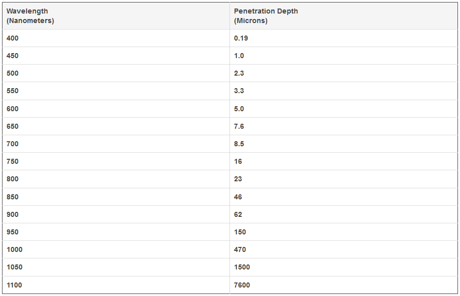
In cases where the photon energy is greater than the band gap energy, an electron has a high probability of being excited into the conduction band, thus becoming mobile. This interaction is also known as the photoelectric effect, and is dependent upon a critical wavelength above which photons have insufficient energy to excite or promote an electron positioned in the valence band and produce an electron-hole pair. When photons exceed the critical wavelength (usually beyond 1100 nanometers), band gap energy is greater than the intrinsic photon energy, and photons pass completely through the silicon substrate. Table 1 lists the depth (in microns) at which 90 percent of incident photons are absorbed by a typical CCD.
Most of the photons with a wavelength between 450 and 700 nanometers are absorbed either in the depletion region or within the bulk material (silicon) of a CCD substrate. Those absorbed into the depletion region with have a quantum efficiency approaching 100 percent, whereas photons entering the substrate generate electrons that experience a three-dimensional random walk and either recombine with holes or diffuse into the depletion region. For those electrons that have negligible diffusion lengths, the quantum efficiency is very low, but those with high diffusion lengths eventually reach a charge well.
Photon Absorption Depth

Table 1
Most CCD arrays utilized in digital cameras designed for scientific applications are sealed within a protected environment to reduce artifacts, improve response, and prolong CCD life. Incoming photons often must pass through a glass or quartz window to reach the pixel array and enter the silicon substrate. Reflection losses at the window surface occur at all photon wavelengths, and transmittance of photons through glass (but not quartz) decreases dramatically for wavelengths below 400 nanometers. Scientific CCD sensors are designed for applications requiring high sensitivity and use quartz coatings to decrease reflection across all wavelengths.
このページはお住まいの地域ではご覧いただくことはできません。